
JP / EN


SOLUTION
SOLUTION
SOLUTION
Production solutions for flat panel and
semiconductor processes
Optopia provides laser production process solutions as an
advanced process technology for flat panel and semiconductor
production processes. Laser-based production process brings
good efficiency, high speed process and high throughput.
LINE BEAM PROCESS
Introduction of line beam component and applications
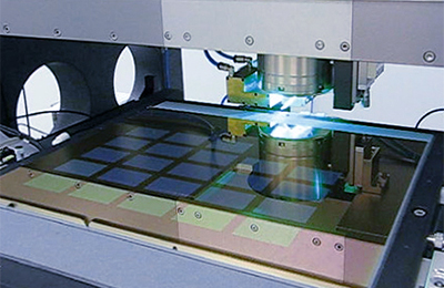
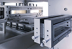
Component of Line beam
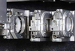
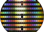
The line beam laser optics consists of a UV solid state laser and a separate line beam optics module. The lasers emitted from the multiple lasers are combined, and are irradiated onto the homogenizer lens array via the collimation optical system. After passing through these optical systems, it is finally condensed by the cylinder imaging optical system to irradiate the substrate with the light of the line beam profile. The maximum length of the line beam irradiated on the substrate is 750mm and the beam width in the minor axis direction is 50μm.

More Information
Laser Lift Off
Laser lift-off is a process that separates a thin film from a glass or crystal substrate. Originally, this technology was used to separate the GaN (gallium nitride) -based compound crystal layer (material layer) for LEDs grown on a sapphire substrate from the sapphire substrate. Applications for flexible display devices and multilayer semiconductor devices are also expanding.
More Information
Laser Annealing
In this process, the surface layer of the amorphous thin film is instantly melted and cooled by a laser to be crystallized and modified into a polyized film. In industrial applications, it is used in the process of modifying amorphous silicon into polysilicon. The ELA performed by the excimer laser was the mainstream, but the system GLA performed by the green solid-state laser with low running cost appeared, and the system UV-SLA that uses the UV solid-state laser that can produce high-performance polysilicon thin film appeared.
More Information
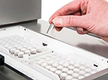
System for Laboratory
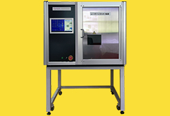
The laser debonding (LDB) process is used to peel off the device formed by the exposure process on the substrate from the backside of the substrate by laser in the flexible display post process, LED manufacturing, and thin film semiconductor process. As long as it is a material that can be ablated, it is possible to peel the interface instantaneously by laser irradiation using a substrate that transmits laser such as glass or sapphire. This device is an experimental device that forms a solid-state UV pulse laser into a line beam and irradiates it onto a substrate.
More Information
OPTICAL MODULE
Optical module for various applications